Nanocrystal SemiConductor for Photovoltaics, Sensor, Heat Reuse
Sponsors
Sponsors
May 6, 2013 – University of Utah metallurgists used an old microwave oven to produce a nanocrystal semiconductor rapidly using cheap, abundant and less toxic metals than other semiconductors. They hope it will be used for more efficient photovoltaic solar cells and LED lights, biological sensors and systems to convert waste heat to electricity.
Using microwaves “is a fast way to make these particles that have a broad range of applications,” says Michael Free, a professor of metallurgical engineering. “We hope in the next five years there will be some commercial products from this, and we are continuing to pursue applications and improvements. It’s a good market, but we don’t know exactly where the market will go.”
Free and the study’s lead author, Prashant Sarswat, a research associate in metallurgical engineering, are publishing their study of the microwaved photovoltaic semiconductor – known as CZTS for copper, zinc, tin and sulfur – in the June 1 issue of the Journal of Crystal Growth.
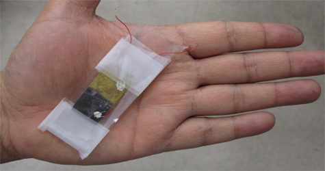
In the study, they determined the optimum time required to produce the most uniform crystals of the CZTS semiconductor – 18 minutes in the microwave oven – and confirmed the material indeed was CZTS by using a variety of tests, such as X-ray crystallography, electron microscopy, atomic force microscopy and ultraviolet spectroscopy. They also built a small photovoltaic solar cell to confirm that the material works and demonstrate that smaller nanocrystals display “quantum confinement,” a property that makes them versatile for different uses.
“It’s not an easy material to make,” Sarswat says. “There are a lot of unwanted compounds that can form if it is not made properly.”
Sarswat says that compared with photovoltaic semiconductors that use highly toxic cadmium and arsenic, ingredients for CZTS photovoltaic material “are more environmentally friendly.”
Free adds: “The materials used for this are much lower cost and much more available than alternatives,” such as indium and gallium often used in semiconductors.
Making an Old Material More Quickly
Swiss researchers first invented CZTS in 1967 using another method. Other researchers discovered in 1998 that it could serve as a photovoltaic material. But until recently, “people haven’t explored this material very much,” Sarswat says. CZTS belongs to a family of materials named quaternary chalcogenides.
Without knowing it at first, Free and Sarswat have been in a race to develop the microwave method of making CZTS with a group of researchers at Oregon State University. Sarswat synthesized the material using microwaves in 2011. Free and Sarswat filed an invention disclosure on their method in January 2012, but the other group beat them into print with a study published in August 2012.
The method developed by Sarswat and Free has some unique features, including different “precursor” chemicals (acetate salts instead of chloride salts) used to start the process of making CZTS and a different solvent (oleylamine instead of ethylene glycol.)
Sarswat says many organic compounds are synthesized with microwaves, and Free notes microwaves sometimes are used in metallurgy to extract metal from ore for analysis. They say using microwaves to process materials is fast and often suppresses unwanted chemical “side reactions,” resulting in higher yields of the desired materials.
CZTS previously was made using various methods, but many took multiple steps and four to five hours to make a thin film of the material, known technically as a “p-type photovoltaic absorber,” which is the active layer in a solar cell to convert sunlight to electricity.
A more recent method known as “colloidal synthesis” – preparing the crystals as a suspension or “colloid” in a liquid by heating the ingredients in a large flask – reduced preparation time to 45 to 90 minutes.
Sarswat decided to try microwave production of CZTS when the University of Utah’s Department of Metallurgical Engineering decided to get a new microwave oven for the kitchen where students heat up their lunches and make coffee.
“Our department secretary had a microwave to throw away,” so Sarswat says he took it to replace one that had recently burned up during other lab experiments.
“The bottom line is you can use just a simple microwave oven to make the CZTS semiconductor,” Free says, adding: “Don’t do it at home. You have to be cautious when using these kinds of materials in a microwave.”
By controlling how long they microwave the ingredients, the metallurgists could control the size of the resulting nanocrystals and thus their possible uses. Formation of CZTS began after 8 minutes in the microwave, but the researchers found they came out most uniform in size after 18 minutes.
Uses for a Microwaved Semiconductor
To make CZTS, salts of the metals are dissolved in a solvent and then heated in a microwave, forming an “ink” containing suspended CZTS nanocrystals. The “ink” then can be painted onto a surface and combined with other coatings to form a solar cell.
“This [CZTS] is the filling that is the heart of solar cells,” says Free. “It is the absorber layer – the active layer – of the solar cell.”
He says the easy-to-make CZTS photovoltaic semiconductor can be used in more efficient, multilayer solar cell designs. In addition, CZTS has other potential uses, according to Sarswat and Free:
– Theromoelectric conversion of heat to electricity, including waste heat from automobiles and industry, or perhaps heat from the ground to power a military camp.
– Biosensors, made by painting the nanocrystal “ink” onto a surface and sensitizing the crystals with an organic molecule that allows them to detect small electrical currents that are created when an enzyme in the body becomes active. These biosensors may play a role in future tests to help diagnose cardiovascular disease, diabetes and kidney disease, Sarswat says.
– As circuit components in a wide variety of electronics, include devices to convert heat to electricity.
– To use solar energy to break down water to produce hydrogen for fuel cells.
The microwave method produced crystals ranging from 3 nanometers to 20 nanometers in size, and the optimum sought by researchers was between 7 nanometers and 12 nanometers, depending on the intended use for the crystals. A nanometer is one-billionth of a meter, or roughly one 25-millionth of an inch.
Larger crystals of CZTS make a good photovoltaic material. Sarswat says the study also demonstrated that smaller crystals of CZTS – those smaller than 5 nanometers – have what is called “quantum confinement,” a change in a material’s optical and electronic properties when the crystals becomes sufficiently small.
Quantum confinement means the nanocrystals can be “tuned” to emit light of specific, making such material potentially useful for a wide variety of uses, including more efficient LEDs or light-emitting diodes for lighting. Materials with quantum confinement are versatile because they have a “tunable bandgap,” an adjustable amount of energy required to activate a material to emit light or electricity.
